How Do Printed Circuit Boards Work?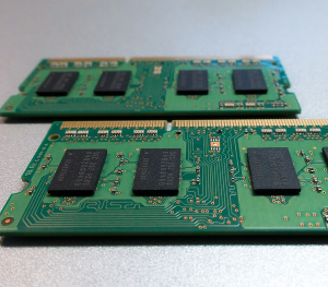
Printed Circuit Boards (PCBs) are used to support and wire the components in many electronic devices. In fact, almost every electronic device available today contains at least one PCB. While many simple electronic devices use single layer PCBs, the PCBs in complex devices may have as many as twelve layers. PCBs provide electricity and connectivity to the parts of an electronic device.
How PCBs Are Made
PCBs are made by mounting components on a non-conductive board. These components are connected by small pathways called traces. In addition to the traces, PCBs have several small holes. These holes allow components to sit flush with the surface of the board.
When creating PCBs, electronic engineers must fit several components on a very small space. Components added to printed circuit boards may include microchips, diodes, registers and switches. The traces connect each of the components and provide them with electricity. These connections are crucial to the proper operation of electronic devices. This is why printed circuit boards are so important to electronic engineering.
The bottom layer of a PCB is non-conductive. The top layer is made from a sheet of metal. The metal layer is printed with etch-resistant ink. It is then etched with special chemicals that remove all but the printed design. The components are then connected through soldering. Thousands of printed circuit boards can be printed at one time.
PCB Design
PCBs are typically designed on a computer. This allows electronic engineers to thoroughly test the PCB before it is produced. It also allows for the ideal arrangement of the parts. After design, the printed circuit board can be printed. PCBs are typically designed with a Computer Aided Design or CAD program. CAD software has replaced the need for manual drafting, which is often inefficient.