Means Engineering, Inc.

Product development engineering in medical, industrial, semiconductor equipment & military with a standard of excellence in form, function and design.

(760) 931-9452 | info@meanseng.com
5927 Geiger Court, Carlsbad, CA 92008-7305

  • Home
  • About Us
    • Our Values
    • Careers
    • Employee Testimonials
    • CMMC Level 3
  • Services
    • Design Engineering
    • Printed Circuit Board
    • Precision Machining
    • High Purity Welding
    • Clean Room Assembly
    • Complex Box Builds
    • Quality Management
  • Featured Works
  • Recent News
  • Resources
    • General Resources
    • Customer Resources
    • Supplier Resources
  • Contact Us

Understanding In-Circuit Testing

March 27, 2020 By cscheafer

Electronics manufacturers must take necessary precautions to ensure nothing goes wrong with finished products. This is especially important for manufacturers creating devices for the medical, aerospace, and defense industries. Even devices made for other industries require careful assembly if manufacturers wish to avoid costly rebuilds, repairs, and recalls.

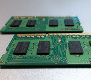
In order to ensure proper operation of all parts and components, electronics manufacturers must continuously test throughout production. Using a wide range of tests at different parts of the process helps ensure the quality and reliability of all finished products.

One of the most commonly used tests, in-circuit testing (ICT), helps ensure contract manufacturers and OEMs consistently meet defined parameters during production. ICT provides valuable information about problems with the board. This can prove extremely beneficial as most issues with electronic devices occur because of short circuits, wrong components, and open circuits on the board.

How it Works

ICT relies on a special test fixture, commonly referred to as “bed of nails” because it contains multiple contact pins. The contact pins come in contact with circuit nodes on the printed circuit board (PCB) to measure performance of the components. ICT allows contract manufacturers to measure various parameters including resistance, capacitance, and the operation of analog components. ICT is also sometimes used to measure functionality of digital circuits. However, full testing of circuit functionality isn’t usually feasible due to circuit complexity.

Benefits of ICT

When performed correctly, ICT can catch around 98% of faults with the board. Test results provided by ICT are easy to interpret. This makes it possible for manufacturers of all skillsets to locate problems quickly. Programming an in circuit tester is extremely easy. Electronics manufacturers can use information provided in the PCB layout to generate most of the program.

Disadvantages of ICT

Although ICT remains one of the most popular printed circuit board testing methods, it’s not without its disadvantages. As the size of components shrink, it’s becoming more difficult for manufacturers to gain access to all nodes on the board. This can lead to unreliable test results.

Contract manufacturers and OEMs must rely on a number of different testing methods to ensure the quality of finished products. This is especially important for those responsible for the creation of potentially life-saving products. Although ICT provides an effecting method for testing PCBs, it’s important that electronics manufacturers use additional tests to determine the quality and reliability of circuit boards.


Filed Under: About Us Tagged With: CM, contract manufacturer, contract manufacturing, electronics manufacturer, ICT, in circuit testing, in-circuit teesting, OEM, PCB, Printed Circuit Board

How Do Printed Circuit Boards Work?

July 21, 2017 By meiadmin

How Do Printed Circuit Boards Work?

Printed Circuit Boards (PCBs) are used to support and wire the components in many electronic devices. In fact, almost every electronic device available today contains at least one PCB. While many simple electronic devices use single layer PCBs, the PCBs in complex devices may have as many as twelve layers. PCBs provide electricity and connectivity to the parts of an electronic device.

How PCBs Are Made

PCBs are made by mounting components on a non-conductive board. These components are connected by small pathways called traces. In addition to the traces, PCBs have several small holes. These holes allow components to sit flush with the surface of the board.

When creating PCBs, electronic engineers must fit several components on a very small space. Components added to printed circuit boards may include microchips, diodes, registers and switches. The traces connect each of the components and provide them with electricity. These connections are crucial to the proper operation of electronic devices. This is why printed circuit boards are so important to electronic engineering.

The bottom layer of a PCB is non-conductive. The top layer is made from a sheet of metal. The metal layer is printed with etch-resistant ink. It is then etched with special chemicals that remove all but the printed design. The components are then connected through soldering. Thousands of printed circuit boards can be printed at one time.

PCB Design

PCBs are typically designed on a computer. This allows electronic engineers to thoroughly test the PCB before it is produced. It also allows for the ideal arrangement of the parts. After design, the printed circuit board can be printed. PCBs are typically designed with a Computer Aided Design or CAD program. CAD software has replaced the need for manual drafting, which is often inefficient.


Filed Under: About Us Tagged With: california, carlsbad, Electronic Devices, Electronics Engineering, electronics manufacturing, PCB, Printed Circuit Board, san diego county, southern california

ABOUT US

MEI features depth of experience in medical, industrial, semiconductor equipment and military products. All product development efforts start with a unique set of requirements, yet we deliver results that share a common standard of excellence in form, function and design.

Our turn-key capabilities provide smart, simple solutions to cumbersome outsourcing issues, and provide our clients with an intelligent route from concept to market.

Read More...

Copyright © 2023 Means Engineering, Inc. · Website by Alter Impact